- 您现在的位置:买卖IC网 > Sheet目录287 > 25LC512-E/MF (Microchip Technology)IC EEPROM 512KBIT 20MHZ 8DFN
�� �
�
�25LC512�
�3.0� PIN� DESCRIPTIONS�
�The� descriptions� of� the� pins� are� listed� in� Table� 3-1.�
�The� WP� pin� function� is� blocked� when� the� WPEN� bit� in�
�the� STATUS� register� is� low.� This� allows� the� user� to�
�install� the� 25LC512� in� a� system� with� WP� pin� grounded�
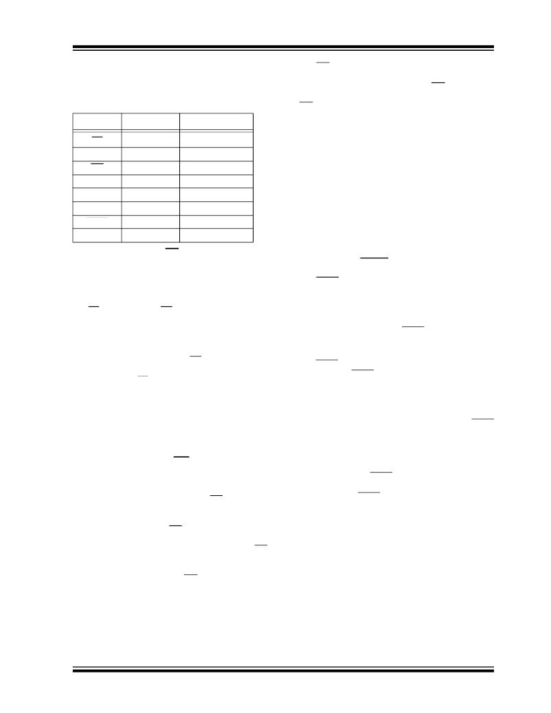
�TABLE� 3-1:�
�PIN� FUNCTION� TABLE�
�and� still� be� able� to� write� to� the� STATUS� register.� The�
�WP� pin� functions� will� be� enabled� when� the� WPEN� bit� is�
�Name�
�Pin� Number�
�Function�
�set� high.�
�CS�
�1�
�Chip� Select� Input�
�3.4�
�Serial� Input� (SI)�
�SO�
�WP�
�2�
�3�
�Serial� Data� Output�
�Write-Protect� Pin�
�The� SI� pin� is� used� to� transfer� data� into� the� device.� It�
�receives� instructions,� addresses� and� data.� Data� is�
�latched� on� the� rising� edge� of� the� serial� clock.�
�V� SS�
�SI�
�4�
�5�
�Ground�
�Serial� Data� Input�
�3.5�
�Serial� Clock� (SCK)�
�SCK�
�HOLD�
�V� CC�
�6�
�7�
�8�
�Serial� Clock� Input�
�Hold� Input�
�Supply� Voltage�
�The� SCK� is� used� to� synchronize� the� communication�
�between� a� master� and� the� 25LC512.� Instructions,�
�addresses� or� data� present� on� the� SI� pin� are� latched� on�
�the� rising� edge� of� the� clock� input,� while� data� on� the� SO�
�3.1� Chip� Select� (CS)�
�A� low� level� on� this� pin� selects� the� device.� A� high� level�
�deselects� the� device� and� forces� it� into� Standby� mode.�
�However,� a� programming� cycle� which� is� already�
�initiated� or� in� progress� will� be� completed,� regardless� of�
�the� CS� input� signal.� If� CS� is� brought� high� during� a�
�program� cycle,� the� device� will� go� into� Standby� mode� as�
�soon� as� the� programming� cycle� is� complete.� When� the�
�device� is� deselected,� SO� goes� to� the� high-impedance�
�state,� allowing� multiple� parts� to� share� the� same� SPI�
�bus.� A� low-to-high� transition� on� CS� after� a� valid� write�
�sequence� initiates� an� internal� write� cycle.� After� power-�
�up,� a� low� level� on� CS� is� required� prior� to� any� sequence�
�being� initiated.�
�pin� is� updated� after� the� falling� edge� of� the� clock� input.�
�3.6� Hold� (HOLD)�
�The� HOLD� pin� is� used� to� suspend� transmission� to� the�
�25LC512� while� in� the� middle� of� a� serial� sequence� with-�
�out� having� to� re-transmit� the� entire� sequence� over�
�again.� It� must� be� held� high� any� time� this� function� is� not�
�being� used.� Once� the� device� is� selected� and� a� serial�
�sequence� is� underway,� the� HOLD� pin� may� be� pulled�
�low� to� pause� further� serial� communication� without�
�resetting� the� serial� sequence.�
�The� HOLD� pin� shoul� d� be� brought� low� while� SCK� is� low,�
�otherwise� the� HOLD� function� will� not� be� invoked� until�
�the� next� SCK� high-to-low� transition.� The� 25LC512� must�
�remain� selected� during� this� sequence.� The� SI� and� SCK�
�3.2�
�Serial� Output� (SO)�
�levels� are� “don’t� cares”� during� the� time� the� device� is�
�paused� and� any� transitions� on� these� pins� w� ill be�
�The� SO� pin� is� used� to� transfer� data� out� of� the� 25LC512.�
�During� a� read� cycle,� data� is� shifted� out� on� this� pin� after�
�the� falling� edge� of� the� serial� clock.�
�ignored.� To� resume� serial� communication,� HOLD�
�should� be� brought� high� while� the� SCK� pin� is� low,� other-�
�wise� serial� communication� will� not� be� resumed� until� the�
�next� SCK� high-to-low� transition.�
�3.3�
�Write-Protect� (WP)�
�The� SO� line� will� tri-state� immediately� upon� a� high-to-�
�This� pin� is� used� in� conjunction� with� the� WPEN� bit� in� the�
�STATUS� register� to� prohibit� writes� to� the� nonvolatile�
�bits� in� the� STATUS� register.� When� WP� is� low� and�
�WPEN� is� high,� writing� to� the� nonvolatile� bits� in� the�
�STATUS� register� is� disabled.� All� other� operations�
�function� normally.� When� WP� is� high,� all� functions,�
�including� writes� to� the� nonvolatile� bits� in� the� STATUS�
�register,� operate� normally.� If� the� WPEN� bit� is� set,� WP�
�low� during� a� STATUS� register� write� sequence� will�
�disable� writing� to� the� STATUS� register.� If� an� internal�
�write� cycle� has� already� begun,� WP� going� low� will� have�
�no� effect� on� the� write.�
�?� 2010� Microchip� Technology� Inc.�
�low� transition� of� the� HOLD� pin,� and� will� begin� outputting�
�again� immediately� upon� a� subsequent� low-to-high�
�transition� of� the� HOLD� pin,� independent� of� the� state� of�
�SCK.�
�DS22065C-page� 19�
�发布紧急采购,3分钟左右您将得到回复。
相关PDF资料
25LC640-E/P
IC EEPROM 64KBIT 2MHZ 8DIP
25LC640A-E/P
IC EEPROM 64KBIT 10MHZ 8DIP
281708-4
PLUG HE14 IDC 90 4 P TUBE
281709-4
PLUG HE13 IDC 90 4 P AWG 24
281711-2
PLUG HE14 IDC 90 2 P TUBE
281783-8
PLUG HE14 IDC 180 8 P AWG 26-24
281784-5
PLUG HE13 IDC 180 5 P AWG 26-24
281786-8
PLUG HE14 IDC 180 8 P AWG 28-26
相关代理商/技术参数
25LC512-E/P
功能描述:电可擦除可编程只读存储器 512k 64KX8 2.5V SER EE EXT RoHS:否 制造商:Atmel 存储容量:2 Kbit 组织:256 B x 8 数据保留:100 yr 最大时钟频率:1000 KHz 最大工作电流:6 uA 工作电源电压:1.7 V to 5.5 V 最大工作温度:+ 85 C 安装风格:SMD/SMT 封装 / 箱体:SOIC-8
25LC512-E/SM
功能描述:电可擦除可编程只读存储器 512k 64KX8 2.5V SER EE EXT RoHS:否 制造商:Atmel 存储容量:2 Kbit 组织:256 B x 8 数据保留:100 yr 最大时钟频率:1000 KHz 最大工作电流:6 uA 工作电源电压:1.7 V to 5.5 V 最大工作温度:+ 85 C 安装风格:SMD/SMT 封装 / 箱体:SOIC-8
25LC512-E/SN
功能描述:电可擦除可编程只读存储器 512k 64KX8 2.5V SER EE EXT RoHS:否 制造商:Atmel 存储容量:2 Kbit 组织:256 B x 8 数据保留:100 yr 最大时钟频率:1000 KHz 最大工作电流:6 uA 工作电源电压:1.7 V to 5.5 V 最大工作温度:+ 85 C 安装风格:SMD/SMT 封装 / 箱体:SOIC-8
25LC512-I/MF
功能描述:电可擦除可编程只读存储器 512k 64KX8 2.5V SER EE IND RoHS:否 制造商:Atmel 存储容量:2 Kbit 组织:256 B x 8 数据保留:100 yr 最大时钟频率:1000 KHz 最大工作电流:6 uA 工作电源电压:1.7 V to 5.5 V 最大工作温度:+ 85 C 安装风格:SMD/SMT 封装 / 箱体:SOIC-8
25LC512-I/P
功能描述:电可擦除可编程只读存储器 512k 64Kx8 2.5V SER EE IND RoHS:否 制造商:Atmel 存储容量:2 Kbit 组织:256 B x 8 数据保留:100 yr 最大时钟频率:1000 KHz 最大工作电流:6 uA 工作电源电压:1.7 V to 5.5 V 最大工作温度:+ 85 C 安装风格:SMD/SMT 封装 / 箱体:SOIC-8
25LC512-I/P
制造商:Microchip Technology Inc 功能描述:SERIAL EEPROM IC
25LC512-I/S16K
功能描述:电可擦除可编程只读存储器 512k, 64K X 8 , 2.5V SER EE IND, DIE in WAFFLE PK RoHS:否 制造商:Atmel 存储容量:2 Kbit 组织:256 B x 8 数据保留:100 yr 最大时钟频率:1000 KHz 最大工作电流:6 uA 工作电源电压:1.7 V to 5.5 V 最大工作温度:+ 85 C 安装风格:SMD/SMT 封装 / 箱体:SOIC-8
25LC512-I/SM
功能描述:电可擦除可编程只读存储器 512k 64KX8 2.5V SER EE IND RoHS:否 制造商:Atmel 存储容量:2 Kbit 组织:256 B x 8 数据保留:100 yr 最大时钟频率:1000 KHz 最大工作电流:6 uA 工作电源电压:1.7 V to 5.5 V 最大工作温度:+ 85 C 安装风格:SMD/SMT 封装 / 箱体:SOIC-8